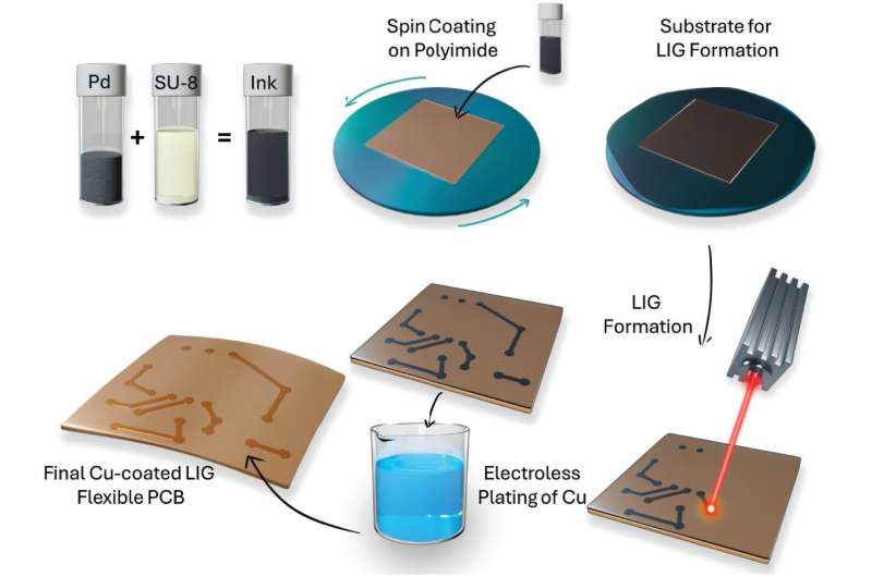
Researchers at Boise State University have introduced a novel method for producing flexible hybrid circuits, aiming to minimize costs and waste while also being mindful of environmental impact. Their findings are highlighted on the cover of Advanced Materials Technologies.
This innovative process utilizes laser-induced graphene, which transforms carbon-based materials into a 3D, conductive, and porous structure through a straightforward laser technique. It’s not only cost-effective but also allows for scalability and precise patterns, making it perfect for electronics, sensors, and energy storage solutions.
In their study, the team employed palladium (Pd) nanoparticles within a polymer base to develop a specialized form of laser-induced graphene. These nanoparticles serve as a foundation for the electroplating of copper, creating essential interconnections for flexible printed circuit boards (f-PCBs) through a laser-assisted manufacturing method.
These interconnections integrate with smaller electronic components, forming a flexible hybrid operational amplifier that can detect changes in resistance during bending. This showcases the technique’s potential in various sensing technologies.
“Using additive manufacturing for printed circuits can enhance electronic production by cutting down on waste, lowering costs, and increasing sustainability,” said Attila Rektor, the lead author of the study. “Our method reduces the need for harmful substances and minimizes material waste, making PCB production more eco-friendly.”
The PCB market worldwide is estimated to be worth about $90 billion USD and is expected to exceed $150 billion USD over the next ten years. This growth is largely driven by the rising demand for flexible PCBs, which offer advantages like compact designs, reduced weight, and improved durability for wearable IoT devices.
“I was excited to see Attila’s work featured on the cover of Advanced Materials Technologies,” remarked Prof. David Estrada from the Micron School of Materials Science and Engineering. “His research effectively connects fundamental scientific discoveries with real-world applications, presenting an innovative way to manufacture flexible PCBs that decreases costs and reduces waste for our industrial partners.”
More information:
Attila Rektor et al, Electroless Plating of Copper on Laser‐Induced Graphene for Flexible Hybrid Electronic Applications, Advanced Materials Technologies (2025). DOI: 10.1002/admt.202401901
If you would like to see similar Tech posts like this, click here & share this article with your friends!

